Contact Us
Overview

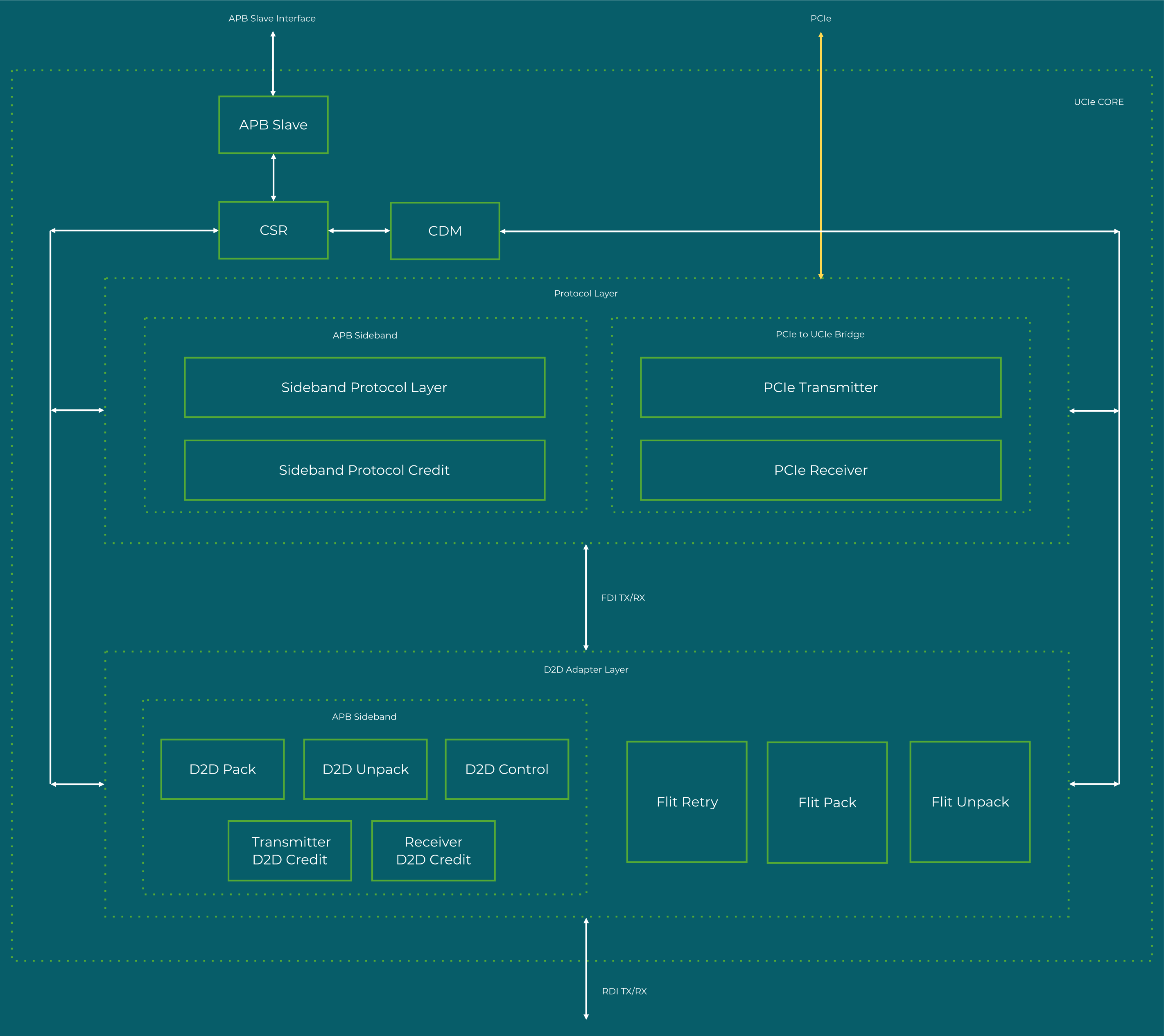
SmartDV’s PCIe to UCIe Bridge IP is a next-generation chiplet interconnect solution engineered for SoC and multi-die system designs requiring seamless, high-bandwidth bridging between PCI Express and Universal Chiplet Interconnect Express fabrics. Fully compliant with UCIe v3.0 and PCI-SIG PCIe 6.0, it enables PCIe protocol traffic to traverse UCIe die-to-die interconnects at speeds up to 64 GT/s, making it a strategic choice for AI accelerators, HPC chiplet systems, and data center multi-die architectures where PCIe-connected chiplets must communicate efficiently across standard and advanced packaging configurations.

As the semiconductor industry accelerates its transition from monolithic SoCs to modular chiplet-based architectures, the need for a standards-compliant PCIe-to-UCIe bridge has become critical. SmartDV’s Bridge IP addresses this with support for both Standard and Advanced Package configurations, all six UCIe FLIT formats, lane widths from 16 to 64 lanes, UCIe clock frequencies from 500 MHz to 8 GHz, and the complete UCIe sideband infrastructure including mailbox messaging, retimer support, and runtime recalibration — giving chiplet system teams a complete, production-ready bridge solution that eliminates the complexity of custom protocol translation.

Built for design flexibility and silicon efficiency, the IP core is highly configurable for both ASIC and FPGA implementations, with a strong focus on area optimization, power management, and peak performance. Its parameterized architecture, configurable clock gating, and clean host interface enable fast integration and confident design bring-up across a wide range of advanced process nodes and chiplet packaging configurations.
Request Data Sheet
PCIe-to-UCIe Bridge
Key Features
  • Full PCIe to UCIe Bridge Functionality – Complete protocol bridge between PCI Express (Root Complex and Endpoint) and UCIe die-to-die interconnect per UCIe v3.0 and PCIe 6.0 specifications
  • Comprehensive UCIe FLIT Format Support – Raw Format, 68B FLIT, Standard 256B End Header, Standard 256B Start Header, Latency-Optimized 256B without Optional Bytes, and Latency-Optimized 256B with Optional Bytes FLIT formats
  • High-Speed Multi-Lane Support – 16, 32, and 64 lane configurations at 4 GT/s through 64 GT/s with UCIe clock frequencies from 500 MHz to 8 GHz for maximum die-to-die bandwidth
  • Standard and Advanced Package Support – Both Standard Package and Advanced Package configurations for flexible 2D and 2.5D chiplet integration
  • Comprehensive Sideband Infrastructure – Sideband messaging for link training and parameter exchange, Sideband Mailbox Mechanism for read/write configuration, 800 MHz sideband data speed, and all Vendor Defined Sideband messages
  • Advanced Link Management – UCIe Retimer support, FLIT Retry Mechanism, FLIT CRC, clock gating, all handshake mechanisms, and Data Link Feature Exchange
  • Multi-Stack Protocol Support – Multi-Stack protocol support for flexible chiplet topology integration across complex multi-die system architectures
  • Full PCIe Controller Support – Complete PCIe 6.0 controller functionality including configurable timers, TLP queuing, multiple Requester/Completer applications, and Retry Mechanism
Compliance and Compatibility
  • Fully compliant with UCIe v3.0 specification (August 2025); backward compatible with UCIe v2.0, v1.1, and v1.0
  • Fully compliant with PCI-SIG PCIe 6.0 specification; backward compatible with PCIe 5.0, 4.0, 3.0, 2.1, 2.0, and 1.0
  • Supports Standard Package and Advanced Package UCIe configurations
  • Configurable SoC interface supporting AXI, AHB, APB, and custom wrappers for seamless integration
  • Compatible with ASIC and FPGA design flows across leading foundry process nodes
  • Compatible with all major EDA synthesis, simulation, and linting flows

Request Datasheet