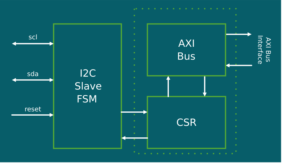
SmartDV’s I2C Slave To AXI Bridge IP is a silicon-proven, fully featured protocol bridge solution purpose-built for SoC designs requiring seamless connectivity between an external I2C controller and an internal AXI-based SoC subsystem across embedded, IoT, and sensor hub applications. Fully compliant with I2C v7.0 (NXP UM10204) on the external interface and ARM AMBA AXI5 on the internal interface, it converts I2C target-side read and write transactions into AXI master transactions, enabling an external I2C host to access internal AXI memory-mapped registers and memory as if it were a native I2C peripheral device.
Designed for the practical integration requirements of modern sensor hub and configuration register access SoC designs, the bridge presents a standards-compliant I2C target on the external bus with 7-bit and 10-bit addressing support, while internally generating AXI master read and write transactions to access the SoC’s internal address space. Its clock stretching support for internal access latency management, configurable I2C target address, and configurable AXI address mapping give embedded SoC teams a production-tested bridge solution for external microcontroller or host processor access to internal SoC registers and memory over a simple two-wire interface.
Built for design flexibility and silicon efficiency, the IP core is highly configurable for both ASIC and FPGA implementations, with a strong focus on area optimization, power management, and peak performance. Its parameterized address mapping and clean integration interface enable fast design bring-up across a wide range of process nodes.