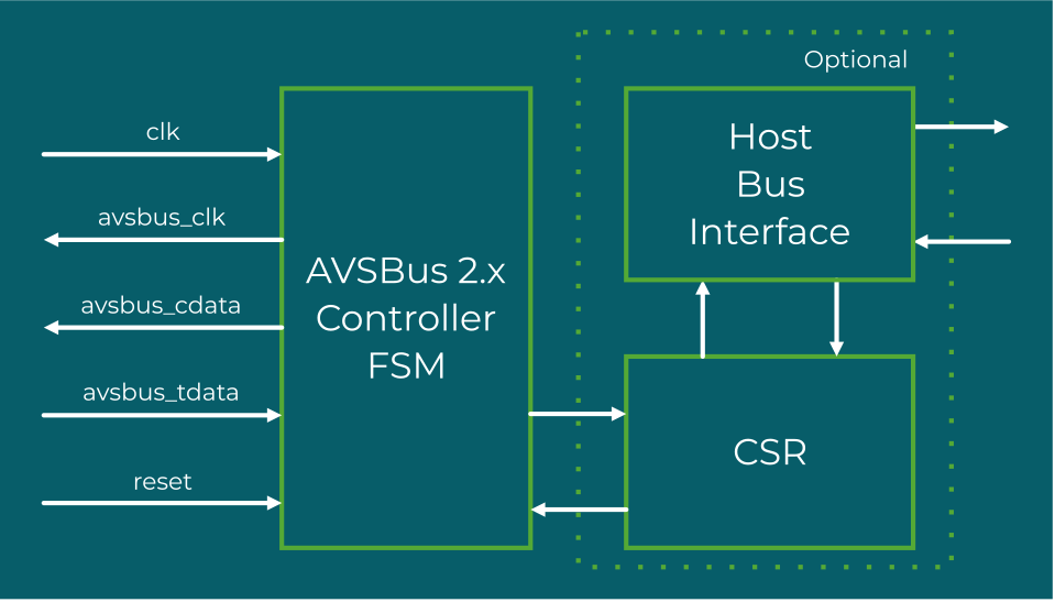
SmartDV’s AVSBus 2.x Master IP is a silicon-proven, fully featured Adaptive Voltage Scaling Bus master solution purpose-built for SoC, ASIC, and FPGA designs requiring next-generation adaptive voltage scaling bus master functionality with multi-slave support and enhanced security. Fully compliant with AVSBus v2.0, the current and latest standalone AVSBus specification published by SMIF, it delivers complete master-side AVSBus functionality with a clean separation from SMBus physical and transport layer constraints, enabling flexible deployment across diverse physical and transport layer configurations while delivering the low-latency voltage control performance demanded by modern high-performance processor and FPGA power management designs.
AVSBus v2.0 represents a significant architectural evolution from v1.3, extending the point-to-point architecture to support multiple slave devices on the bus, adding enhanced security within the digital power communication domain, and providing a clear separation between AVSBus command sets and the underlying SMBus physical and transport layers for greater deployment flexibility. SmartDV’s AVSBus 2.x Master IP implements the complete v2.0 feature set giving SoC and power management teams a production-tested, spec-complete master implementation ready for the most demanding next-generation adaptive voltage scaling system designs.
Built for design flexibility and silicon efficiency, the IP core is highly configurable for both ASIC and FPGA implementations, with a strong focus on area optimization, power management, and peak performance. Its broad SoC bus interface support and clean host interface enable fast integration and confident design bring-up across a wide range of process nodes and target applications.