Contact Us
Overview

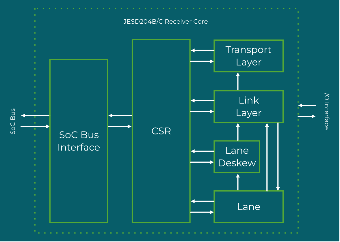
SmartDV’s JESD204B/C Receiver IP is a silicon-proven, fully featured serial interface receiver solution purpose-built for SoC designs requiring reliable, standards-compliant high-speed data converter connectivity across RF, instrumentation, wireless infrastructure, and test and measurement applications. Fully compliant with JESD204C.1 and backward compatible with JESD204B, it delivers complete receiver functionality supporting Subclass 0, 1, and 2, 1 to 8 lanes, and 1 to 64 converters per receiver, with support for both Multiple-Converter Device Alignment Multiple-Lanes (MCDA-ML) topologies.

Designed for the demanding requirements of modern data converter interface receivers, the IP supports frame sizes of 1, 2, 4, 8, and 16 octets per frame, HD-mode, 1 to 32-bit data width per converter, configurable control words per frame clock period, 0 to 3 control bits per sample, 1 to 8 samples per converter, and 1 to 32 frames per multiframe. Its support for 4, 8, 12, 16, 20, 24, 28, and 32 bits per sample, 0 to 15 bank ID extension to DID, 0 to 255 device identification numbers, 0 to 7 lane identification numbers, and different SerDes interfaces from 10 to 60 bits and custom bit widths give RF and instrumentation SoC teams a production-tested, spec-complete JESD204B/C receiver implementation.

Built for design flexibility and silicon efficiency, the IP core is highly configurable for both ASIC and FPGA implementations, with a strong focus on area optimization, power management, and peak performance. Its parameterized lane and converter architecture and clean host interface enable fast integration across a wide range of RF and data converter process nodes.
Request Data Sheet
JESD204BC Receiver
Key Features
  • Full JESD204B/C Receiver Functionality – Complete receiver implementation compliant with JESD204C.1, backward compatible with JESD204B, supporting Subclass 0, 1, and 2
  • Flexible Lane and Converter Configuration – 1 to 8 lanes with 1 to 64 converters per receiver for scalable data converter interface designs
  • Comprehensive Frame Configuration – Frame sizes of 1, 2, 4, 8, and 16 octets with HD-mode, 1 to 32-bit data width per converter, and 1 to 32 frames per multiframe
  • Flexible Sample and Control Configuration – 4 to 32 bits per sample, 0 to 3 control bits per sample, 1 to 8 samples per converter, and configurable control words per frame clock period
  • Device Identification Support – 0 to 15 bank ID extension to DID, 0 to 255 device identification numbers, and 0 to 7 lane identification numbers
  • Flexible SerDes Interface – Support for 10, 20, 40, and 60-bit SerDes interfaces plus custom bit widths per lane
  • Error Statistics Reporting – Comprehensive reporting of various error statistics for link health monitoring
  • MCDA-ML Support – Multiple-Converter Device Alignment, Multiple-Lanes device topology support
Compliance and Compatibility
  • Fully compliant with JEDEC JESD204C.1 (December 2021); backward compatible with JESD204B and JESD204C
  • Supports Subclass 0, 1, and 2 timing modes
  • Configurable SoC interface supporting AMBA AXI, AHB, APB, and custom wrappers for seamless integration
  • Compatible with ASIC and FPGA design flows across leading foundry process nodes
  • Compatible with all major EDA synthesis, simulation, and linting flows

Request Datasheet