Contact Us
Overview

SmartDV’s SLVS-EC Verification IP is a comprehensive solution for verifying Scalable Low Voltage Signaling with Embedded Clock, the Sony Semiconductor Solutions developed and JIIA standardized high-speed serial interface connecting CMOS Image Sensors to Digital Signal Processors in industrial, machine vision, and high-resolution imaging applications. Fully compliant with SLVS-EC Specification Version 3.1 and backward compatible with Versions 3.0, 2.0, and 1.2, it supports complete verification of SLVS-EC Transmitter and Receiver devices across Basic, Multiple I/F, and Multiple CIS system topologies, all four defined frame synchronization schemes, multi-lane configurations from 1 to 8 lanes, RAW 8, 10, 12, 14, and 16-bit color formats, embedded data transfer, and multiple stream transfer.

SmartDV’s SLVS-EC VIP supports UVM, SystemVerilog, and Verilog, and integrates seamlessly into diverse verification environments. It is simulator-independent and compatible with all leading EDA simulators, providing flexibility across simulation platforms.

With LINK and PHY protocol management, 8B/10B encoding and decoding, Gigabit Channel Coding (GCC) for reduced overhead transmission, Forward Error Correction, Error Correction Code, Cyclic Redundancy Check, skew and jitter insertion, comprehensive error injection and detection, built-in functional coverage, and a complete test suite, SmartDV’s SLVS-EC VIP enables verification teams to thoroughly validate SLVS-EC interface designs for industrial cameras, machine vision systems, automotive imaging, and high-resolution, high-frame-rate CMOS image sensor applications.
Request Data Sheet
SLVS-EC VIP
Key Features
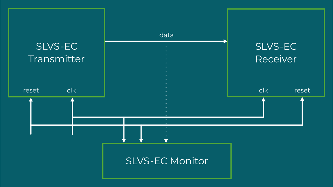
  • Full SLVS-EC Transmitter and Receiver Support – Provides complete SLVS-EC Transmitter device and Receiver device verification across Basic Topology, Multiple I/F Topology, and Multiple CIS Topology system configurations between CIS and DSP, and all four defined frame synchronization schemes including DSP Master with and without shared clock, and CIS Master with and without shared clock.
  • Multi-Lane and Baud Rate Coverage – Supports multi-lane configurations of 1, 2, 4, 6, and 8 lanes, and all defined baud grades including Baud Grade 1 at 1152 to 1250 Mbps, Baud Grade 2 at 2304 to 2500 Mbps, and Baud Grade 3 at 4608 Mbps and above, covering the full range of SLVS-EC v3.1 high-speed lane rates.
  • Data Format and Transfer Mode Coverage – Supports RAW 8, 10, 12, 14, and 16-bit color formats, embedded data transfer, and multiple stream transfer for verification of complex multi-stream image sensor data paths including full-resolution video combined with still image capture.
  • Advanced Encoding and Error Correction – Supports 8B/10B encoding and decoding, Gigabit Channel Coding (GCC) as introduced in SLVS-EC v3.0/3.1 for reduced-overhead transmission compared to conventional 8b/10b, Forward Error Correction (FEC), Error Correction Code (ECC), and Cyclic Redundancy Check (CRC) for comprehensive data integrity verification.
  • LINK and PHY Protocol Management – Supports complete LINK Protocol Management and PHY Protocol Management covering all defined protocol layer behaviors, with skew insertion and jitter insertion for robust physical layer signal integrity verification.
  • Comprehensive Error Injection and Detection – Detects and reports all defined SLVS-EC error types including invalid control character, disparity error, invalid 10-bit code, sync errors, truncated packet, illegal standby/config, insufficient blanking, delayed line end, line boundary error, and bandwidth misarrangement.
  • Complete Verification Infrastructure – Provides a full test suite covering all SLVS-EC v3.1 specification features, built-in functional coverage analysis, status counters for bus events, and callbacks in node transmitter, receiver, and monitor for user-defined data processing and protocol and timing violation notification.
Compliance and Compatibility
  • Fully compliant with SLVS-EC Specification Version 3.1; backward compatible with Versions 3.0, 2.0, and 1.2
  • Standardized by the Japan Industrial Imaging Association (JIIA), developed by Sony Semiconductor Solutions
  • Supports lane rates up to 12.5 Gbps/lane across 1, 2, 4, 6, and 8 lane configurations
  • Supports Gigabit Channel Coding (GCC) and 8B/10B encoding with FEC, ECC, and CRC
  • Compatible with UVM, OVM, VMM, SystemVerilog, and Verilog verification environments
  • Compatible with all major EDA simulators including Synopsys VCS, Cadence Xcelium, Siemens Questa, Aldec Riviera-PRO, and Verilator

Request Datasheet