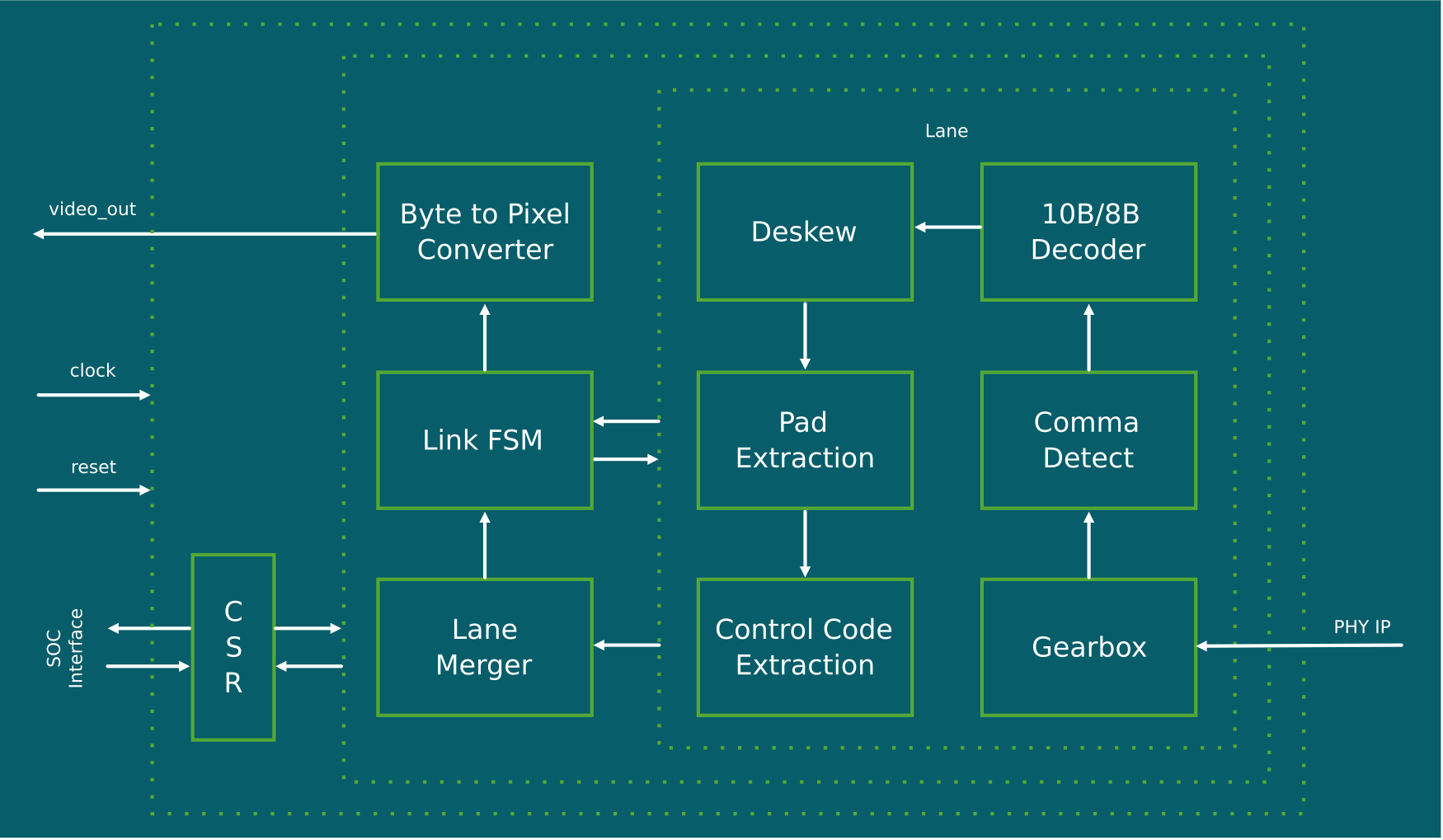
SmartDV’s SLVS-EC Receiver IP is a silicon-proven, fully featured Scalable Low Voltage Signaling with Embedded Clock receiver solution purpose-built for DSP and FPGA host SoC designs requiring reliable, high-speed reception of image sensor data from SLVS-EC compliant CMOS image sensors. Fully compliant with JIIA SLVS-EC v3.0 and backward compatible with v2.0, it delivers complete receiver-side SLVS-EC functionality supporting up to 8 lanes at data rates from 1152 Mbps through 5000 Mbps across Baud Grades 1, 2, and 3, making it a production-ready image sensor receiver for high-resolution, high-frame-rate camera systems in automotive ADAS, industrial vision, and consumer camera applications.
Designed to address the demanding image data reception requirements of modern camera subsystem designs, the IP supports all standard CIS-DSP system topologies including Basic, Multiple I/F, and Multiple CIS configurations, hardware lane deskew for reliable multi-lane data alignment, multiple color formats from RAW8 through RAW16, embedded data reception, and multiple stream support. Its comprehensive 11-type error detection suite covering invalid control characters, disparity errors, sync errors, packet integrity, and bandwidth misarrangements gives DSP and FPGA SoC teams a production-tested, spec-complete SLVS-EC receiver that handles the widest range of image sensor configurations with maximum protocol compliance.
Built for design flexibility and silicon efficiency, the IP core is highly configurable for both ASIC and FPGA implementations, with a strong focus on area optimization, power management, and peak performance. Its parameterized lane architecture, hardware deskew, and clean host interface enable fast integration and confident design bring-up across a wide range of advanced imaging process nodes and target applications.