Contact Us
Overview

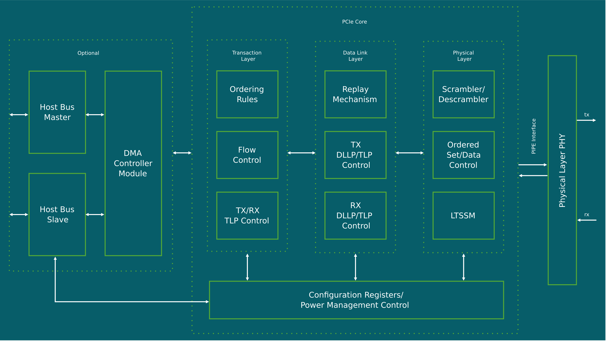
SmartDV’s PCIe 5.0 Controller IP is a high-performance PCI Express interconnect solution purpose-built for SoC designs requiring extreme bandwidth connectivity across AI/ML accelerators, high-performance computing, and next-generation data center applications. Fully compliant with the PCI-SIG PCIe 5.0 specification, it delivers complete Root Complex and Endpoint controller functionality at 32 GT/s per lane with 128b/130b encoding and support for link widths up to x16, providing a feature-complete PCIe interconnect foundation capable of up to 128 GB/s bidirectional throughput in an x16 configuration.

Engineered for the extreme bandwidth and signal integrity demands of AI accelerator and HPC interconnect designs, the IP implements the complete LTSSM state machine, data scrambling, full link speed and width negotiation, and a comprehensive transaction layer supporting up to 8 Virtual Channels and 8 Traffic Classes. Currently FPGA proven and targeting silicon validation, it gives SoC teams early access to a spec-complete PCIe 5.0 controller implementation for platform bring-up and system validation ahead of production deployment.

Built for design flexibility and silicon efficiency, the IP core is highly configurable for both ASIC and FPGA implementations, with a strong focus on area optimization, power management, and peak performance. Its PIPE interface compatibility, up to 40-bit SerDes width support, and comprehensive power management feature set enable fast integration and confident design bring-up across a wide range of advanced process nodes and target applications.
Request Data Sheet
PCIe Controller
Key Features
  • Full PCIe 5.0 Root Complex and Endpoint Support – Complete controller implementation per PCI-SIG PCIe 5.0 specification at 32 GT/s with 128b/130b encoding and support for link widths up to x16
  • Complete LTSSM State Machine – Full Link Training and Status State Machine with speed and link width negotiation, lane polarity inversion, lane reversal detection and correction, and data scrambling
  • Comprehensive Transaction Layer – Up to 8 Virtual Channels with configurable depth queuing, up to 8 Traffic Classes, configurable TC to VC mapping, and multi-function support
  • Robust Data Integrity – LCRC, DLLP field checking, TLP header and prefix validation, ECRC support, and retry mechanism for reliable high-speed data transfer
  • Advanced Power Management – ASPM, software-controlled power management, Link Power Management, L1 PM Sub-states, and Emergency Power Reduction State support
  • Lane Margining at Receiver – Hardware lane margining support for improved signal integrity validation at 32 GT/s operating speeds
  • High-Performance SerDes Interface – Up to 40-bit SerDes width support and configurable fixed Pclk/fixed data path implementation for flexible high-speed PHY integration
Compliance and Compatibility
  • Fully compliant with PCI-SIG PCIe 5.0 specification; backward compatible with PCIe 4.0, 3.1, 3.0, 2.1, 2.0, and 1.0
  • Supports PIPE interface for PHY integration
  • Configurable SoC interface supporting AXI, AHB, APB, and custom wrappers for seamless integration
  • Compatible with ASIC and FPGA design flows across leading foundry process nodes
  • Compatible with all major EDA synthesis, simulation, and linting flows

Request Datasheet