Contact Us
Overview

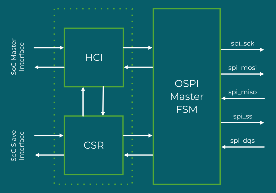
SmartDV’s Octal SPI Master IP is a silicon-proven, high-performance serial peripheral interface solution purpose-built for SoC designs requiring flexible, high-bandwidth connectivity to Octal SPI flash memories and other serial peripheral devices across embedded, automotive, IoT, and high-performance computing applications. Compliant with the JEDEC xSPI standard (JESD251C) and the SPI de-facto standard, it delivers complete master-side Octal SPI functionality at clock frequencies up to 133 MHz with support for Single, Dual, Quad, and Octal data line configurations, providing a scalable, backward-compatible serial interface solution for a wide range of flash and peripheral connectivity requirements.

Designed for the practical integration requirements of modern SoC designs, the IP supports up to 16 slave devices, full duplex operation, configurable FIFO depths, software-programmable CPOL and CPHA transmission formats, and both LSB and MSB data ordering. Its support for 8, 16, 24, and 32-bit synchronous serial transmission widths, software-programmable SCLK rate, fast sampling clock input, and interrupt-driven operation give SoC teams a production-tested, feature-complete Octal SPI master that adapts to the specific requirements of each target application.

Built for design flexibility and silicon efficiency, the IP core is highly configurable for both ASIC and FPGA implementations, with a strong focus on area optimization, power management, and peak performance. Its parameterized FIFO architecture, configurable slave select management, and clean host interface enable fast integration and confident design bring-up across a wide range of process nodes and target applications.
Request Data Sheet
Octal SPI Master
Key Features
  • Full Octal SPI Master Functionality – Complete master-side implementation supporting Single, Dual, Quad, and Octal serial data line configurations for flexible, scalable serial peripheral connectivity
  • High-Speed Operation – Clock frequencies up to 133 MHz with fast sampling clock input for high-bandwidth serial flash and peripheral access
  • Multi-Slave Support – Up to 16 slave devices under master control for flexible multi-device SPI bus topologies
  • Flexible Transmission Formats – Software-programmable CPOL and CPHA settings, LSB and MSB data ordering, and 8, 16, 24, and 32-bit synchronous serial transmission widths
  • Full Duplex Operation – Simultaneous transmit and receive for maximum SPI bus utilization
  • Configurable FIFO Architecture – Configurable depth TX and RX FIFOs for efficient data transfer management across varying bandwidth requirements
  • Software-Programmable SCLK Rate – Flexible clock rate configuration for adaptation to diverse slave device timing requirements
  • Interrupt Control – Programmable interrupt generation for efficient, event-driven SPI transfer management
Compliance and Compatibility
  • Compliant with JEDEC xSPI standard JESD251C
  • Compliant with SPI de-facto standard including CPOL/CPHA modes 0, 1, 2, and 3
  • Backward compatible with Quad SPI, Dual SPI, and standard SPI interfaces
  • Configurable SoC interface supporting AMBA AXI, AHB, APB, and custom wrappers for seamless integration
  • Compatible with ASIC and FPGA design flows across leading foundry process nodes
  • Compatible with all major EDA synthesis, simulation, and linting flows

Request Datasheet