Contact Us
Overview

SmartDV’s GDDR5/5X Verification IP is a comprehensive solution for verifying Graphics Double Data Rate memory interfaces for high-bandwidth GPU, AI accelerator, networking, and compute applications. Fully compliant with JEDEC JESD212C (GDDR5) and JESD232A (GDDR5X), it supports complete verification of GDDR5 and GDDR5X device components across x16 and x32 device configurations with densities up to 8 GB, covering all defined commands, mode register programming, training modes, CRC-8 error detection, data and address bus inversion, low power modes, and all timing and protocol violation detection for both GDDR5 and GDDR5X operating modes.

SmartDV’s GDDR5/5X VIP supports UVM, SystemVerilog, and Verilog, and integrates seamlessly into diverse verification environments. It is simulator-independent and compatible with all leading EDA simulators, providing flexibility across simulation platforms.

With comprehensive support for DDR data via WCK, SDR command via CK, DDR addressing, programmable burst length, read and write latency, on-die termination, auto and self-refresh, built-in functional coverage, and a complete test suite, SmartDV’s GDDR5/5X VIP enables verification teams to thoroughly validate graphics memory interface designs for discrete GPUs, AI accelerators, automotive graphics, and high-performance networking SoC applications.
Request Data Sheet
GDDR5/5X VIP
Key Features
  • Full GDDR5 and GDDR5X Device Support – Supports complete GDDR5 device verification per JESD212C and GDDR5X device verification per JESD232A across x16 and x32 device configurations, densities up to 8 GB, all defined commands, and programmable clock frequency of operation for both standards.
  • GDDR5X High-Speed and Extended Prefetch Support – Supports GDDR5X data rates from 10 to 14 Gb/s with 64-byte prefetch architecture doubling GDDR5’s 32-byte prefetch, pseudo open drain signaling consistent with GDDR5 for smooth transition, and all GDDR5X-specific mode register extensions and timing parameters.
  • Comprehensive Signal Interface Support – Supports single-ended interface for command, address, and data, Double Data Rate data via WCK clock, Single Data Rate command via CK clock, Double Data Rate addressing via CK clock, and all defined GDDR5 and GDDR5X physical interface configurations.
  • Training and Calibration Support – Covers address training, input/output PLL and DLL operation, CRC-8 cyclic redundancy check with programmable CRC read and write latency, write data mask function via address bus, data bus inversion, and address bus inversion for complete interface training and calibration verification.
  • Power Management and Refresh Support – Supports all low power operating modes, auto refresh and self-refresh modes, auto precharge option for each burst access, input clock stop and frequency change, and on-die termination for all high-speed inputs.
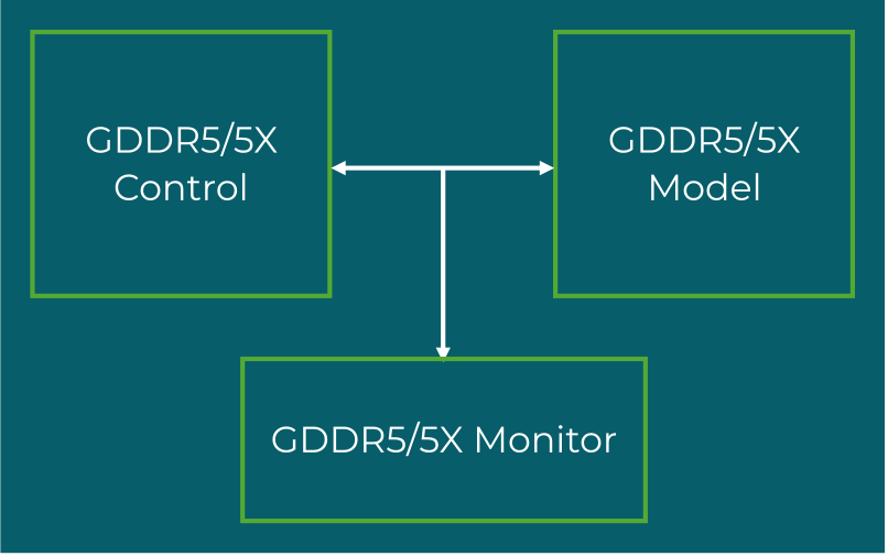
  • Comprehensive Protocol Checking – Provides continuous monitoring of GDDR5 and GDDR5X device behavior during simulation, covering power-on, initialization, power-off rules, state-based rules, active command rules, read and write command rules, and all timing violations, with protocol checkers fully compliant with JESD212C and JESD232A.
  • Complete Verification Infrastructure – Provides built-in functional coverage analysis, constraints randomization, and callbacks for user access to monitor-observed data across all GDDR5 and GDDR5X protocol conditions.
Compliance and Compatibility
  • Fully compliant with JEDEC JESD212C (GDDR5 SGRAM); backward compatible with JESD212C.01 and JESD212
  • Fully compliant with JEDEC JESD232A (GDDR5X SGRAM)
  • Supports x16 and x32 device configurations with densities up to 8 GB
  • Compatible with UVM, OVM, VMM, SystemVerilog, and Verilog verification environments
  • Compatible with all major EDA simulators including Synopsys VCS, Cadence Xcelium, Siemens Questa, Aldec Riviera-PRO, and Verilator

Request Datasheet