Contact Us
Overview

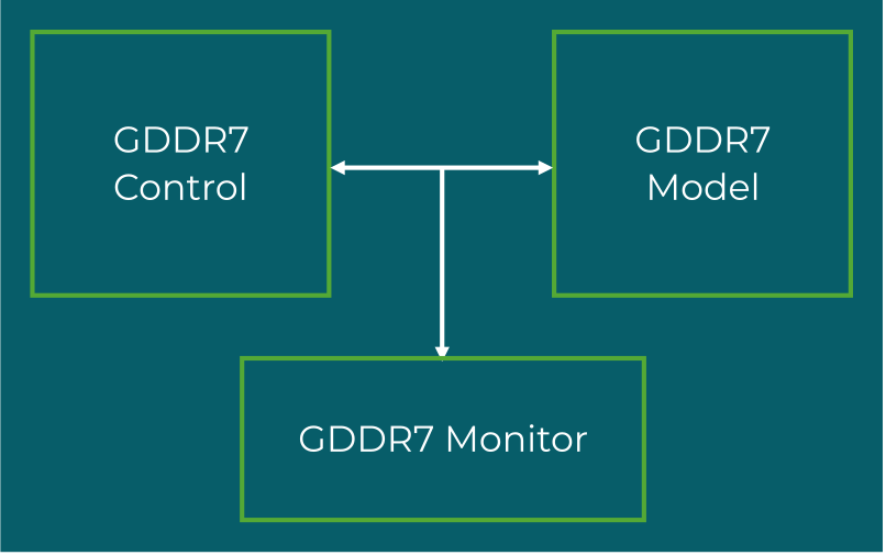
SmartDV’s GDDR7 Verification IP is a comprehensive solution for verifying Graphics Double Data Rate 7 memory interfaces, the first JEDEC graphics DRAM standard to adopt PAM3 signaling for high-frequency, high-bandwidth operation. Fully compliant with JEDEC JESD239E and backward compatible with JESD239D and JESD239.01, it supports complete verification of GDDR7 device components across x8 device configurations with four independent channels and densities from 16 Gb to 128 Gb, covering all defined commands, PAM3 high-speed and NRZ low-speed data signaling, four-channel and two-channel mode operation, comprehensive RAS features including on-die ECC, data poison, CA parity with command blocking, and all defined training modes, refresh management, and power management features.

SmartDV’s GDDR7 VIP supports UVM, SystemVerilog, and Verilog, and integrates seamlessly into diverse verification environments. It is simulator-independent and compatible with all leading EDA simulators, providing flexibility across simulation platforms.

With comprehensive PAM3 signaling verification, LFSR-based training with eye masking and error counters, Adaptive and Directed Refresh Management, post package repair, Dynamic Voltage Sequence support, bus-accurate timing for all timing delay ranges, built-in functional coverage, and a complete test suite, SmartDV’s GDDR7 VIP enables verification teams to thoroughly validate next-generation graphics memory interface designs for discrete GPUs, AI training and inference accelerators, cloud gaming, high-performance computing, and networking SoC applications.
Request Data Sheet
GDDR7 VIP
Key Features
  • Full GDDR7 Device Support – Supports complete GDDR7 device verification per JEDEC JESD239E across x8 device mode, four independent channel point-to-point interface configurations for data, Command Address, and clocks, densities from 16 Gb to 128 Gb, all defined GDDR7 commands, and 4-channel and 2-channel mode configuration set at power-up via CA0_A and CA0_C.
  • PAM3 High-Speed and NRZ Low-Speed Signaling – Supports high-speed data signaling using PAM3 three-level pulse amplitude modulation transmitting 3 bits over 2 cycles for significantly improved data rate and SNR over traditional NRZ, NRZ low-speed data signaling option, single-ended and differential Read clock per channel, and ERR signal (PAM3 coded) for communicating WRCRC and CAPAR errors.
  • Four-Channel Architecture and Bank Group Support – Supports four separate independent channels with point-to-point interface, Double Data Rate data bus with respect to WCK, Single Data Rate CA bus with NRZ input supporting single and multicycle commands, bank grouping with 16 internal banks per channel, burst length of 16 symbols in PAM3 mode and 32 in NRZ mode, and auto precharge option for each burst access.
  • Comprehensive RAS and Data Integrity – Supports on-die ECC with real-time reporting, data poison, CA parity (CAPAR) and CA parity with command blocking (CAPARBLK), READ/WRITE CRC on/off mode, read/write data transmission integrity via cyclic redundancy check, DBI and CABI, programmable DQE latency and WRCRC2ERR latency, and Info Read for device identification and status information.
  • Comprehensive Training Mode Support – Covers Command Address Bus Training, ERR signal training, FIFO Data Training Mode, LFSR Data Training Mode with PRBS 11 or 15 and programmable seed, Read Training, Write Training, Command Address Oscillator training, and Duty Cycle Corrector training, with READ FIFO pattern preload by LDFF command and CA Oscillator support.
  • Refresh Management and Power States – Supports Refresh Management, Adaptive RFM, and Directed RFM, auto refresh with 16k cycles and all-bank and per-bank options, self refresh, Sleep, Self Refresh Sleep, and Hibernate Self Refresh Sleep modes, Temperature Controlled Self Refresh rate, frequency change sequence, Dynamic Voltage Sequence support including FDMR, and CSP command and feedback for Sleep to synchronous operation.
  • Post Package Repair and Advanced Features – Supports hard Post Package Repair (hPPR), on-die termination operation, programmable READ/WRITE latency, input/output PLL/DLL, power down features, input clock stop and frequency change, and Vendor ID support via all mode register programming.
  • Comprehensive Protocol CheckingProvides continuous bus-accurate monitoring of GDDR7 device behavior during simulation for minimum, maximum, and typical timing values, covering power-on, initialization, power-off rules, state-based rules, active command rules, read and write command rules, and all timing violations, with protocol checker fully compliant with JEDEC JESD239E.
  • Complete Verification Infrastructure – Provides built-in functional coverage analysis, constraints randomization, and callbacks for user access to command data and monitor-observed data across all GDDR7 protocol conditions.
Compliance and Compatibility
  • Fully compliant with JEDEC JESD239E (GDDR7 SGRAM); backward compatible with JESD239D and JESD239.01
  • Supports x8 device mode with densities from 16 Gb to 128 Gb
  • Supports PAM3 high-speed and NRZ low-speed signaling
  • Compatible with UVM, OVM, VMM, SystemVerilog, and Verilog verification environments
  • Compatible with all major EDA simulators including Synopsys VCS, Cadence Xcelium, Siemens Questa, Aldec Riviera-PRO, and Verilator

Request Datasheet