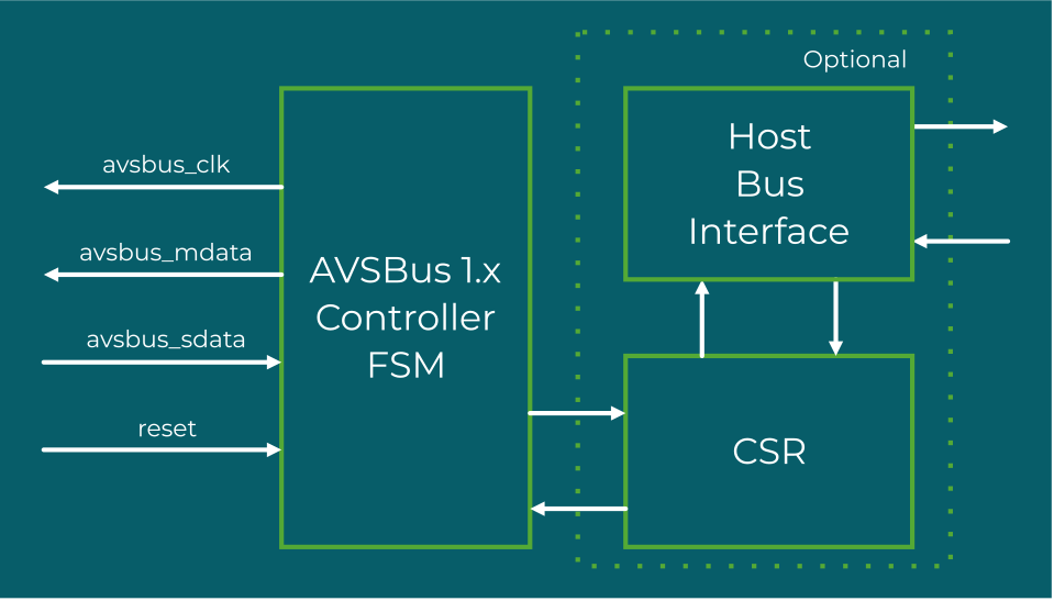
SmartDV’s AVSBus 1.x Master IP is a silicon-proven, fully featured Adaptive Voltage Scaling Bus master solution purpose-built for SoC, ASIC, and FPGA designs requiring fast, deterministic point-to-point voltage control communication with Point of Load voltage regulators. Fully compliant with AVSBus v1.3 (PMBus Part III), it delivers complete master-side AVSBus functionality over a two-wire or three-wire SPI-like interface at bus speeds up to 50 MHz, enabling adaptive voltage scaling with sub-microsecond command latency for power-optimized processor and FPGA voltage rail management.
Designed as a high-speed complement to PMBus for voltage scaling applications, the IP supports all AVSBus commands and data types, clock resynchronization, clock suspension, master alert generation, back-to-back command support, user response frames, status response handling, timeout detection, and frame alignment. Its simple three-wire interface with AVS_MData, AVS_SData, and AVS_Clock signals minimizes integration complexity while delivering the low-latency voltage change commands needed for effective adaptive voltage scaling in modern high-performance SoC designs.
Built for design flexibility and silicon efficiency, the IP core is highly configurable for both ASIC and FPGA implementations, with a strong focus on area optimization, power management, and peak performance. Its broad SoC bus interface support and clean host interface enable fast integration and confident design bring-up across a wide range of process nodes and target applications.