Contact Us
Overview

SmartDV’s LPDDR5/5X Verification IP is a comprehensive solution for verifying Low Power Double Data Rate 5 and LPDDR5X memory interfaces across device and PHY interface implementations. Fully compliant with JEDEC JESD209-5C covering both LPDDR5 and the LPDDR5X optional extension and backward compatible with JESD209-5B, JESD209-5A, and JESD209-5, and DFI versions 2.0 through 5.0, it supports complete verification of LPDDR5 and LPDDR5X device components across x8 and x16 device configurations with densities up to 32 GB, covering all defined commands, 2:1 and 4:1 CKR modes, BG, 8B, and 16B bank organization modes, all training modes, refresh management, CA parity, ECC, and the DDR PHY Interface across DDR3, DDR4, DDR5, LPDDR3, LPDDR4, and LPDDR5 memory protocols.

SmartDV’s LPDDR5/5X VIP supports UVM, SystemVerilog, and Verilog, and integrates seamlessly into diverse verification environments. It is simulator-independent and compatible with all leading EDA simulators, providing flexibility across simulation platforms.

With comprehensive WCK2CK sync, deep sleep, frequency set point operation, hybrid refresh, refresh credit mode, data copy low power function, write clock free running mode, partial array self-refresh segment masking, DFI multi-protocol support, bus-accurate timing, built-in functional coverage, and a complete test suite, SmartDV’s LPDDR5/5X VIP enables verification teams to thoroughly validate LPDDR5 and LPDDR5X memory subsystem designs for flagship smartphones, 5G platforms, automotive ADAS, AR/VR, edge AI, and power-sensitive high-bandwidth computing applications.
Request Data Sheet
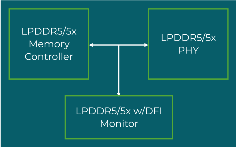
LPDDR5/5x with DFI VIP
Benefits
  • Complete LPDDR5 and LPDDR5X Device Protocol Coverage – Supports 100% of the LPDDR5 protocol standard across JESD209-5C, JESD209-5B, JESD209-5A, and JESD209-5, including the LPDDR5X optional extension for higher bandwidth and simplified architecture, all LPDDR5 commands, x8 and x16 device configurations, densities up to 32 GB, all defined data rates up to 8533 Mbps, burst lengths of 16 and 32, programmable read/write latencies, and programmable clock frequency of operation.
  • Advanced Architecture and Bank Organization – Supports 2:1 and 4:1 CKR clock to WCK ratio modes, BG bank group, 8B, and 16B bank organization modes, multi-rank configurations, byte mode, all mode register programming, write DBI and read DBI operation, write data mask operation, and WCK2CK sync operation for complete LPDDR5 and LPDDR5X interface architecture verification.
  • Comprehensive Training Mode Support – Covers command bus training, WCK2CK leveling, WCK-DQ training, and enhanced RDQS training mode, along with CA parity and ECC verification for complete LPDDR5 interface training and data integrity verification.
  • Advanced Refresh and Power Management – Supports optimized refresh, Refresh Management Command, Adaptive and Directed Refresh Management, hybrid refresh mode, refresh credit mode, partial array self-refresh segment masking, power down mode, self-refresh operation, deep sleep mode, frequency set point operation, and input clock stop and frequency change for thorough power management verification.
  • Advanced LPDDR5 Feature Coverage – Supports write clock free running mode, data copy low power function, write X operation, single-ended mode, multi-rank operation, and all LPDDR5X-specific higher bandwidth and simplified architecture features as defined in JESD209-5C.
  • Multi-Protocol DFI Interface Support – Compliant with DFI versions 2.0 through 5.0 supporting DDR3, DDR4, DDR5, LPDDR3, LPDDR4, and LPDDR5 memory protocols across all DFI interface groups, with 1:1, 1:2, and 1:4 MC to PHY frequency ratios, write transactions with DBI, DM, and CRC, read transactions with DBI, per-slice read leveling, CA training, write leveling, frequency change protocol, gear down mode, WCK control interface for LPDDR5, and PHY-independent training mode as per DFI 5.0.
  • Comprehensive Protocol Checking – Provides continuous bus-accurate monitoring of LPDDR5 and LPDDR5X device behavior during simulation for minimum, maximum, and typical timing values, covering power-on, initialization, power-off rules, state-based rules, active command rules, read and write command rules, and all timing violations, with protocol checker fully compliant with JESD209-5C.
  • Complete Verification Infrastructure – Provides built-in functional coverage analysis, constraints randomization, all mode register programming support, and callbacks for user access to command data and monitor-observed data across all LPDDR5, LPDDR5X, and DFI protocol conditions.
Compliance and Compatibility
  • Fully compliant with JEDEC JESD209-5C (LPDDR5/5X); backward compatible with JESD209-5B, JESD209-5A, and JESD209-5
  • Supports LPDDR5X optional extension for higher bandwidth operation up to 8533 Mbps
  • Supports x8 and x16 device configurations with densities up to 32 GB
  • Compliant with DFI versions 2.0, 2.1, 3.0, 3.1, 4.0, and 5.0
  • DFI protocol support covers DDR3, DDR4, DDR5, LPDDR3, LPDDR4, and LPDDR5
  • Compatible with UVM, OVM, VMM, SystemVerilog, and Verilog verification environments
  • Compatible with all major EDA simulators including Synopsys VCS, Cadence Xcelium, Siemens Questa, Aldec Riviera-PRO, and Verilator

Request Datasheet