Contact Us
Overview

SmartDV’s LPDDR5 Controller IP is a silicon-proven, high-performance memory controller solution purpose-built for mobile, automotive, and AI-driven SoCs requiring ultra-high-bandwidth, low-power access to LPDDR5 and LPDDR5X memory devices. Fully compliant with JEDEC JESD209-5C and DFI v5.0 specifications, it delivers industry-leading memory bandwidth and low-latency access with support for device densities up to 32GB across x8 and x16 device configurations and all LPDDR5 speed grades up to 6400 MT/s.

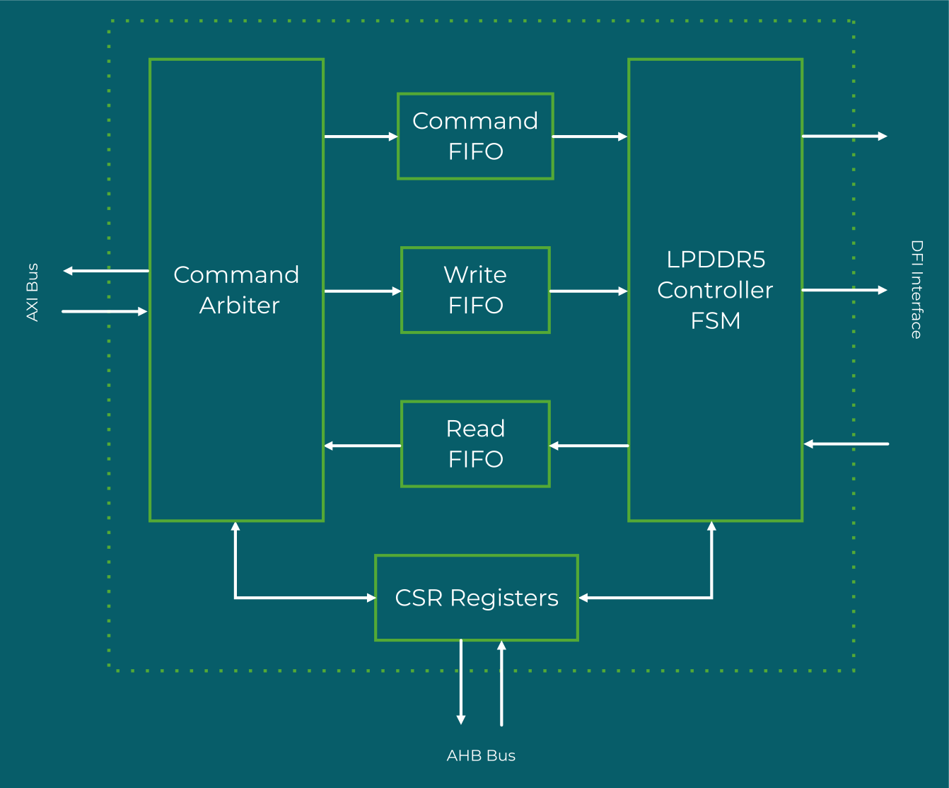
Engineered to meet the extreme bandwidth and power demands of 5G, AI inference, and advanced automotive workloads, the controller delivers a comprehensive LPDDR5 feature set including WCK2CK synchronization, Frequency Set Point operation, advanced refresh management with hybrid and credit modes, and an extensive training suite covering Command Bus Training, WCK2CK leveling, WCK-DQ training, and Enhanced RDQS training. Its QoS-based multi-port arbitration, transaction reordering, and support for up to 16 AXI ports with data widths up to 512 bits ensure optimal throughput across the most demanding concurrent memory access scenarios.

Built for design flexibility and silicon efficiency, the IP core is highly configurable for both ASIC and FPGA implementations, with a strong focus on area optimization, power management, and peak performance. Its parameterized architecture, programmable page policy, 2:1 and 4:1 clock ratio mode support, and flexible host interface options enable fast integration and confident design bring-up across a wide range of process nodes and target applications.
Request Data Sheet
LPDDR5 Controller
Benefits
  • Full LPDDR5 Command Support – Complete implementation of all LPDDR5 commands per JEDEC JESD209-5C including BG, 8B, and 16B bank organization modes
  • High-Bandwidth Multi-Port AXI Interface – Up to 16 AXI ports with data widths up to 512 bits, QoS-based in-port arbitration, and controllable outstanding transactions for maximum memory bandwidth
  • Advanced Refresh Management – Optimized Refresh, Adaptive and Directed Refresh Management, hybrid refresh mode, refresh credit mode, and partial array self-refresh segment masking
  • WCK Support – WCK2CK synchronization, WCK Control, and write clock free-running mode for reliable high-speed clocking
  • Comprehensive Training Suite – Command Bus Training, WCK2CK leveling, WCK-DQ training, and Enhanced RDQS training for robust high-speed memory bring-up
  • Advanced Data Integrity – Read and Write DBI, CRC for read and write operations, and Command Address Parity for reliable high-speed data transfer
  • Comprehensive Power Management – Deep Sleep, Self Refresh, Power Down, Frequency Set Point operation, and data copy low power function for power-optimized mobile and automotive operation
  • High-Capacity Multi-Rank Support – Up to 32GB device density with x8 and x16 configurations, multi-rank support, and all LPDDR5 speed grades
  • Built-In Self-Test – Integrated memory BIST for full address range testing and identification of damaged memory locations
  • Flexible Clock and Burst Control – Programmable burst lengths of 16 and 32, 2:1 and 4:1 clock ratio modes, and 1:4 controller to DFI PHY frequency ratio
Compliance and Compatibility
  • Fully compliant with JEDEC JESD209-5C (LPDDR5/LPDDR5X); backward compatible with JESD209-5B and JESD209-5A
  • Compliant with DFI v5.0 specification
  • Configurable SoC interface supporting AXI, AHB, APB, and custom wrappers for seamless integration
  • Supports x8 and x16 LPDDR5 device configurations up to 32GB density
  • Compatible with ASIC and FPGA design flows across leading foundry process nodes
  • Compatible with all major EDA synthesis, simulation, and linting flows

Request Datasheet