Contact Us
Overview

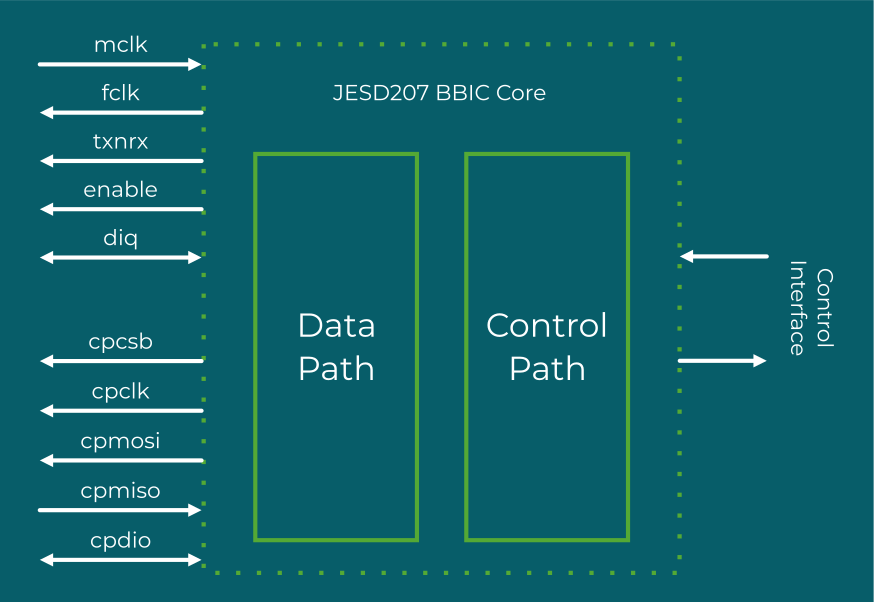
SmartDV’s JESD207 BBIC IP is a silicon-proven, high-performance baseband interface solution engineered for wireless SoC applications requiring reliable, high-speed data exchange between baseband integrated circuits (BBIC) and radio front-end transceivers (RFIC). Fully compliant with the JEDEC JESD207 specification, it implements the complete RF-BB Digital Parallel (RBDP) interface, supporting both data path transactions and control plane transactions for seamless BBIC-to-RFIC connectivity.

Designed for the demanding requirements of modern wireless systems, the IP core supports 1T1R, 1T2R, and 2T2R configurations alongside flexible interleaving and parallel data width options, making it well-suited for a broad range of radio access technologies and antenna configurations. Its power-efficient control plane architecture, with clock gating between transactions, makes it an ideal choice for power-sensitive wireless applications where control plane power consumption is critical.

Built for design flexibility and silicon efficiency, the IP core is highly configurable for both ASIC and FPGA implementations, with a strong focus on area optimization, power management, and peak performance. Its parameterized architecture and flexible host interface options enable fast integration and confident design bring-up across a wide range of process nodes and wireless SoC applications.
Request Data Sheet
JESD207 BBIC
Key Features
  • Full JESD207 BBIC Functionality – Complete baseband-side data path and control plane implementation per JEDEC JESD207 specification
  • Flexible Antenna Configuration Support – 1T1R, 1T2R, and 2T2R system configurations for broad wireless application coverage
  • High-Speed DDR Data Transfer – Half-duplex DDR source synchronous data transfer timing for efficient, high-bandwidth RF-BB data exchange
  • Configurable Parallel Data Width – Supports 12, 14, and 16-bit parallel data widths with 2-way and 4-way interleave transactions
  • Multiple Parallel Sample Stream Support – Simultaneous transmission and reception of multiple parallel sample streams for advanced MIMO and carrier aggregation use cases
  • Power-Efficient Control Plane – Serial clock gating between transactions reduces control plane power consumption to negligible levels
  • Comprehensive Control Plane Support – 4-wire and 3-wire read/write transactions with extended data transaction support and 1-bit command plus 7-bit address field format
Compliance and Compatibility
  • Fully compliant with JEDEC JESD207 specification
  • Configurable SoC interface supporting AMBA AXI, AHB, APB, and custom wrappers for seamless integration
  • Compatible with ASIC and FPGA design flows across leading foundry process nodes
  • Compatible with all major EDA synthesis, simulation, and linting flows

Request Datasheet