Contact Us
Overview

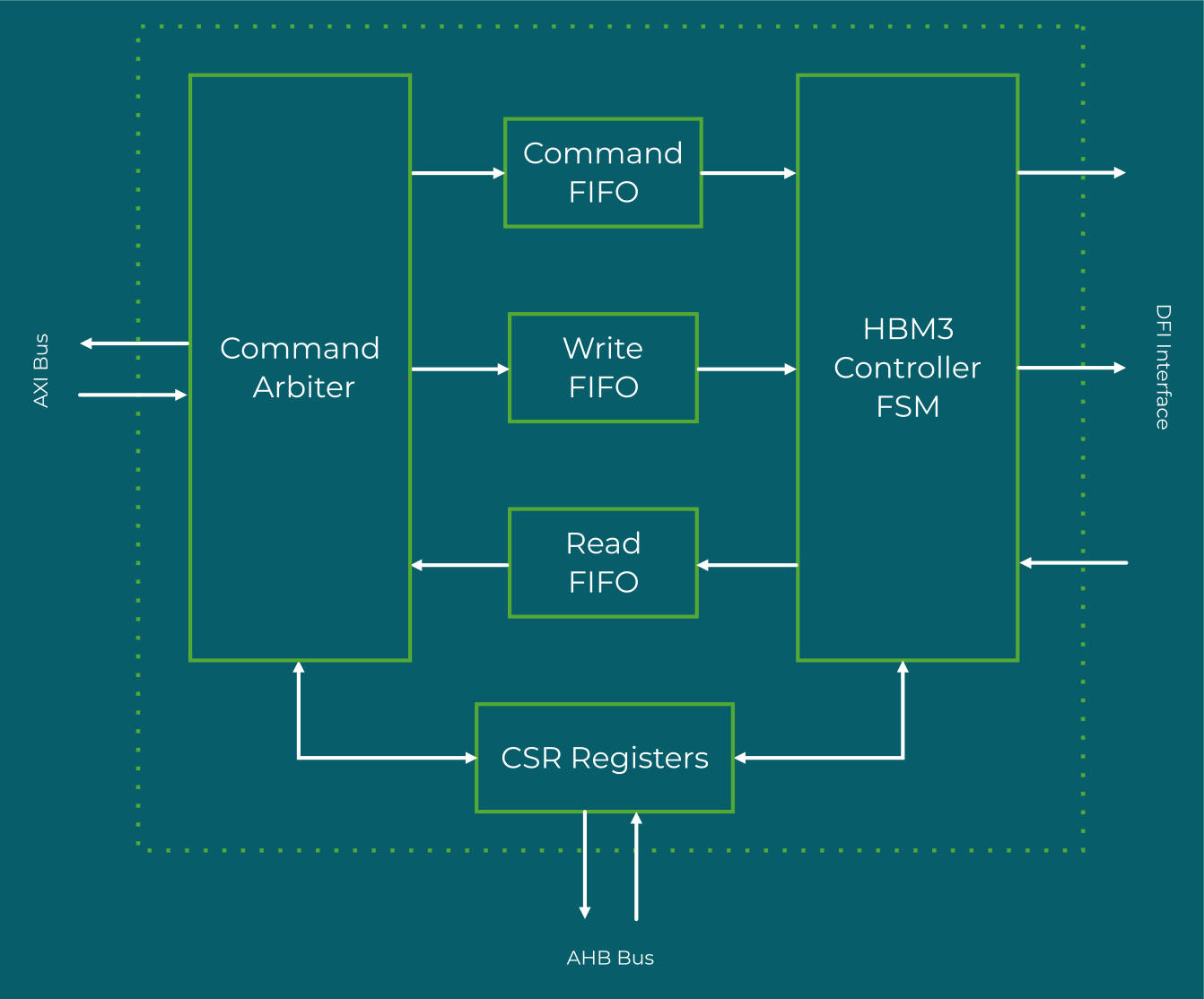
SmartDV’s HBM3 Controller IP is a fully featured High Bandwidth Memory controller solution purpose-built for SoC designs requiring the highest available memory bandwidth across AI/ML accelerator, GPU, and high-performance computing applications. Supporting JEDEC HBM3 per JESD238 and JESD238A and compliant with DFI v4.0 or v5.0, it delivers complete controller functionality supporting up to 16 AXI ports with data widths up to 512 bits, data rates up to 6.4 Gb/s per pin, and up to 16 channels per stack with two pseudo channels each for virtually 32 channels of independent access.

Designed to maximize memory bandwidth in the most demanding AI and HPC SoC designs, the IP supports configurable open and closed page policies, transaction reordering, in-port and multi-port arbitration, burst length of 8, bank grouping across up to 64 banks per pseudo channel, semi-independent row and column command interfaces, and 1:4, 1:2, and 1:1 Controller to DFI PHY frequency ratios. Its Command/Address and Data parity, WDQS-to-CK training, Data Bus Inversion (DBIac), Pseudo Channel Mode operation, and IEEE 1500 support give AI and HPC SoC teams a production-tested, spec-complete HBM3 controller for the highest-bandwidth memory subsystem designs in the industry.

Built for design flexibility and silicon efficiency, the IP core is highly configurable for both ASIC and FPGA implementations, with a strong focus on area optimization, power management, and peak performance. Its parameterized AXI port count and bus-accurate timing model for min, max, and typical values enable fast integration across a wide range of AI and HPC process nodes.
Request Data Sheet
HBM3 Controller
Key Features
  • Full HBM3 Controller Functionality – Complete controller per JESD238 and JESD238A supporting data rates up to 6.4 Gb/s per pin and channel densities of 2GB to 32GB
  • High-Performance AXI Interface – Up to 16 AXI ports with data widths up to 512 bits, in-port and multi-port arbitration, and transaction reordering
  • Massive Channel Parallelism – Up to 16 channels per stack with 2 pseudo channels per channel for virtually 32 channels of independent memory access
  • Semi-Independent Command Interfaces – Semi-independent row and column command interfaces for maximum command throughput
  • HBM3 Data Integrity – Command/Address parity and Data parity support alongside Data Bus Inversion (DBIac) for write and read
  • WDQS-to-CK Training – Complete WDQS-to-CK training support for reliable high-speed data strobe alignment
  • Flexible Frequency Ratios – 1:4, 1:2, and 1:1 Controller to DFI PHY frequency ratio support for flexible clocking architectures
  • Comprehensive Power Management – DRAM Clock disabling, Low power control features, self-refresh modes, and power down support
  • IEEE 1500 Support – IEEE Standard 1500 support for embedded core test access
  • Bus-Accurate Timing – Bus-accurate timing model for min, max, and typical values across the full HBM3 command set
Compliance and Compatibility
  • Compliant with JEDEC HBM3 JESD238 and JESD238A specifications
  • Compliant with DFI v4.0 or v5.0 specification
  • Configurable SoC interface supporting AMBA AXI with up to 16 ports and custom wrappers
  • Compatible with ASIC and FPGA design flows across leading foundry process nodes
  • Compatible with all major EDA synthesis, simulation, and linting flows

Request Datasheet