Contact Us
Overview

SmartDV’s DDR4 Verification IP is a comprehensive solution for verifying DDR4 SDRAM memory interfaces across device, 3D Stacked, DIMM module, Data Buffer, Registering Clock Driver, and PHY interface implementations. Fully compliant with JEDEC JESD79-4 through JESD79-4D for DDR4 devices and the DDR4 3DS addendum, JESD82-31A for the DDR4 RCD, JESD82-32A for the DDR4 Data Buffer, and DFI versions 2.0 through 5.0, it provides complete verification coverage across DDR4 standalone devices supporting densities up to 16 GB, DDR4 UDIMM, RDIMM, and LRDIMM module types supporting densities up to 64 GB, DDR4 3DS, RCD01 and RCD02 registering clock driver components, Data Buffer with all training modes, and the DDR PHY Interface across DDR3, DDR4, DDR5, LPDDR3, LPDDR4, and LPDDR5 memory protocols.

SmartDV’s DDR4 VIP supports UVM, SystemVerilog, and Verilog, and integrates seamlessly into diverse verification environments. It is simulator-independent and compatible with all leading EDA simulators, providing flexibility across simulation platforms.

With full on-the-fly protocol and data checking, comprehensive training mode coverage across all DDR4 components, NVDIMM feature support, DFI multi-protocol coverage, bus-accurate timing for all timing delay ranges, built-in functional coverage, and a complete test suite, SmartDV’s DDR4 VIP enables verification teams to thoroughly validate DDR4 memory subsystem designs for server, networking, storage, automotive, and high-performance computing applications.
Request Data Sheet
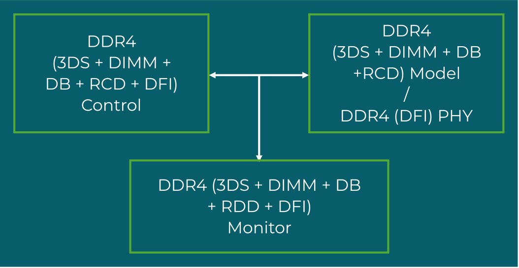
DDR4 (3DS + DIMM + DB + RCD + DFI)
Key Features
  • Complete DDR4 Device Protocol Coverage – Supports 100% of the DDR4 protocol standard across JESD79-4 through JESD79-4D, all DDR4 commands, x4, x8, x16, and x32 device widths, densities up to 16 GB, all speed grades, programmable write and read latency, programmable burst lengths of 4 and 8, sequential and interleaved burst types, programmable preamble, and read preamble training.
  • Comprehensive DDR4 Device Feature Support – Covers all mode register programming, data mask and Data Bus Inversion, write leveling and ZQ calibration, Fine Granularity Refresh Mode, DQ Vref training, CRC for write operations, DLL, Command Address Parity, Post Package Repair, Control Gear Down Mode, CAL Mode Operation, Per DRAM Addressability, Connectivity Test mode, MBIST PPR, synchronous and asynchronous ODT, power down, Maximum Power Saving mode, and input clock stop and frequency change.
  • DDR4 3DS Protocol Coverage – Supports 100% of the DDR4 3DS protocol standard across JESD79-4-1, JESD79-4-1A, and JESD79-4-1B, all DDR4 3DS commands, x4 and x8 device widths, densities up to 16 GB, all speed grades, programmable write and read latency, programmable burst lengths of 4 and 8, programmable preamble, read preamble training, sequential and interleaved burst types, all mode register programming, data mask and Data Bus Inversion, write leveling and ZQ calibration, Fine Granularity Refresh Mode, DQ Vref training, CRC for write operations, DLL, Command Address Parity, Post Package Repair, Control Gear Down Mode, CAL Mode Operation, Per DRAM Addressability, Connectivity Test mode, synchronous and asynchronous ODT, power down, Maximum Power Saving mode, and input clock stop and frequency change.
  • DDR4 DIMM Module Support – Supports 100% of the DDR4 DIMM protocol standard across UDIMM, RDIMM, and LRDIMM types with densities up to 64 GB, x4, x8, and x16 device widths, 16 internal banks, single, dual, and quad rank configurations, ECC error detection and correction, fly-by topology, address mirroring, parity operations, Low Power Auto Self Refresh, Data Bus Inversion, fixed burst chop of 4 and burst length of 8, and BC4 or BL8 on-the-fly selection.
  • DDR4 Registering Clock Driver (RCD) Support – Supports 100% of the DDR4 RCD protocol standard JESD82-31A including all DDR4 command and address bus transactions, parity, Direct CS, Quad CS, and Encoded Quad CS operating modes, dual frequency, register CKE and clock stopped power down modes, output inversion, latency equalization, output delay and slew rate control, transparent mode, Control Gear Down Mode, CA bus training, multi-purpose register, all control word programming, and optional NVDIMM save and restore mode entry and exit sequences.
  • DDR4 Data Buffer (DB) SupportSupports 100% of the DDR4 DB protocol standard JESD82-32A and JESD79-4B including all Data Buffer commands, all speed grades, data buffer power down modes, dual frequency, parity checking, command sequence error detection and handling, read commands and MPR override reads, Per DRAM and Per Buffer Addressability, BCW write and read commands, function spaces F0 through F7, transparent mode, and all training modes including DRAM interface write leveling, host interface write leveling, DRAM-to-DB read delay training, DB-to-DRAM write delay training, host interface read training, and host interface write training.
  • Multi-Protocol DFI Interface Support – Compliant with DFI versions 2.0 through 5.0 supporting DDR3 JESD79-3F, DDR4 JESD79-4D, DDR5 JESD79-5, LPDDR3 JESD209-3C, LPDDR4 JESD209-4B, and LPDDR5 JESD209-5 memory protocols across all DFI interface groups, with 1:1, 1:2, and 1:4 MC to PHY frequency ratios, write transactions with DBI, DM and CRC, read transactions with DBI, frequency change protocol, CA parity signaling, DRAM clock disabling, gear down and 2N mode, 3D stack support, WCK control interface for LPDDR5, and PHY-independent training mode as per DFI 5.0.
  • Comprehensive Protocol Checking and Monitoring – Provides continuous on-the-fly protocol and data checking across all DDR4 components, bus-accurate timing for minimum, typical, and maximum values, comprehensive timing and protocol violation detection covering power up, initialization, power off, state-based rules, active command rules, read and write command rules, and all timing violations, with protocol checkers fully compliant with JESD79-4 through JESD79-4D, JESD82-31A, JESD82-32A, and DFI 2.0 through 5.0 specifications.
Compliance and Compatibility
  • Fully compliant with JEDEC JESD79-4 through JESD79-4D (DDR4 SDRAM)
  • Fully compliant with JEDEC JESD79-4-1, JESD79-4-1A, and JESD79-4-1B (DDR4 3DS)
  • Supports DDR4 UDIMM, RDIMM, and LRDIMM module types
  • Fully compliant with JEDEC JESD82-31A (DDR4 RCD)
  • Fully compliant with JEDEC JESD82-32A (DDR4 Data Buffer)
  • Compliant with DFI versions 2.0, 2.1, 3.0, 3.1, 4.0, and 5.0
  • DFI protocol support covers DDR3, DDR4, DDR5, LPDDR3, LPDDR4, and LPDDR5
  • Compatible with UVM, OVM, VMM, SystemVerilog, and Verilog verification environments
  • Compatible with all major EDA simulators including Synopsys VCS, Cadence Xcelium, Siemens Questa, Aldec Riviera-PRO, and Verilator

Request Datasheet