Contact Us
Overview

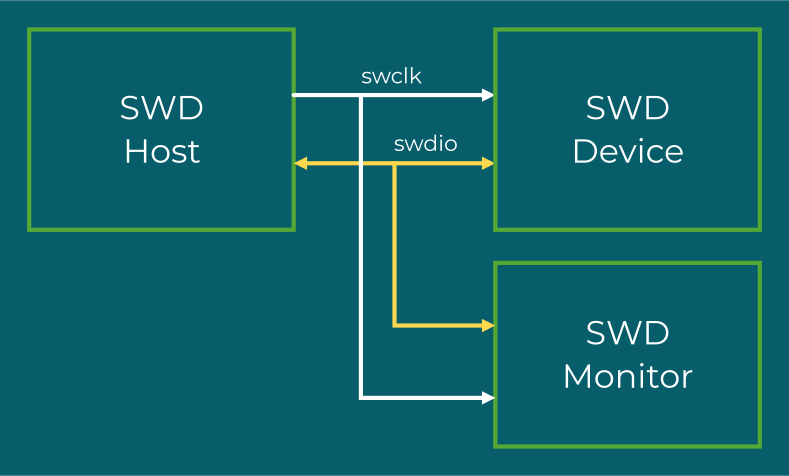
SmartDV’s SWD Verification IP is a comprehensive solution for verifying the ARM Serial Wire Debug interface, the two-pin low-pin-count alternative to JTAG used for accessing debug and trace resources on ARM-based systems-on-chip. Fully compliant with the ARM Debug Interface Architecture Specification ADIv6.0 and backward compatible with ADIv5.0 through ADIv5.2, it supports complete verification of SWD Host and Device components across a single bidirectional SWDIO data connection with separate SWCLK clock, synchronous data transfer, START and STOP bit generation and handling, Debug Port (DP) and Access Port (AP) register accessing, and multidrop SWD supporting multiple Debug Ports on a single bus as introduced in ADIv6.

SmartDV’s SWD VIP supports UVM, SystemVerilog, and Verilog, and integrates seamlessly into diverse verification environments. It is simulator-independent and compatible with all leading EDA simulators, providing flexibility across simulation platforms.

With WAIT and FAULT response handling, Line Reset, Header and Data parity generation and checking, Sticky Overrun behavior, SW-DP write buffering, comprehensive error injection, built-in functional coverage, and a complete test suite, SmartDV’s SWD VIP enables verification teams to thoroughly validate SWD interface designs for ARM-based microcontrollers, application processors, debug probes, and any SoC requiring low-pin-count on-chip debug and trace access.
Request Data Sheet
SWD VIP
Key Features
  • Full SWD Host and Device Support – Provides complete SWD Host and Device component verification across a single bidirectional data connection with a separate synchronous clock, START and STOP bit generation and handling, and complete Debug Port (DP) and Access Port (AP) register accessing for all defined memory-mapped and debug register transactions.
  • Multidrop SWD Coverage – Supports multidrop SWD as introduced in ADIv6, allowing multiple Debug Ports to share a single SWD bus, for verification of multi-DP topologies on systems requiring access to multiple independent debug domains over a shared physical interface.
  • Response and Recovery Handling – Supports WAIT response handling for read or write operation requests, FAULT response handling for read or write operation requests, Line Reset for protocol resynchronization, and Sticky Overrun behavior for robust error state management across the SWD link.
  • Parity and Data Integrity Coverage – Supports Header and Data parity generation and Header and Data parity error checks for complete request and data phase integrity verification, along with SW-DP write buffering for verification of buffered write transaction behavior.
  • Comprehensive Error Injection and Detection – Supports insertion of errors on Stop bit, Park bit, and random Write NACK insertion by Device for thorough protocol violation and fault tolerance verification across all defined SWD transaction phases.
  • Complete Verification Infrastructure – Provides a full test suite covering all ARM SWD specification features, built-in functional coverage analysis, and callbacks in Host and Device for user-defined event handling and protocol and timing violation notification.
Compliance and Compatibility
  • Fully compliant with ARM Debug Interface Architecture Specification ADIv6.0 (ARM IHI 0074D); backward compatible with ADIv5.0 through ADIv5.2 (ARM IHI 0031G)
  • Supports multidrop SWD for multiple Debug Ports on a single bus
  • Supports DPACC and APACC register access transactions
  • Compatible with UVM, OVM, VMM, SystemVerilog, and Verilog verification environments
  • Compatible with all major EDA simulators including Synopsys VCS, Cadence Xcelium, Siemens Questa, Aldec Riviera-PRO, and Verilator

Request Datasheet