Contact Us
Overview

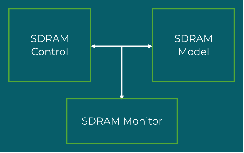
SmartDV’s SDRAM Verification IP is a comprehensive solution for verifying Synchronous Dynamic Random Access Memory controller interfaces, providing accurate SDR SDRAM device models for SoC and FPGA designs requiring embedded memory simulation. Compliant with the JEDEC JESD21-C Section 3.11 SDR SDRAM standard and the Hynix HY57V56820FT-H 512Mb SDR SDRAM device specification, it supports complete verification of SDR SDRAM controller and device interactions across programmable burst lengths from 1 to full page, all refresh modes, internal bank management, all mode register programming, auto-precharge including concurrent auto-precharge, power-up, initialization, and power-off sequencing, and all defined timing parameters for speed grades -7E and -75.

SmartDV’s SDRAM VIP supports UVM, SystemVerilog, and Verilog, and integrates seamlessly into diverse verification environments. It is simulator-independent and compatible with all leading EDA simulators, providing flexibility across simulation platforms.

With bus-accurate timing for minimum, maximum, and typical values, comprehensive protocol checking covering all state-based rules, command rules, and timing violations, continuous bus monitoring, built-in functional coverage, and callbacks for user data access, SmartDV’s SDRAM VIP enables verification teams to thoroughly validate SDR SDRAM controller interface designs for embedded processors, FPGAs, SoCs, DSPs, and any application using synchronous DRAM for main memory or frame buffer storage.
Request Data Sheet
SDRAM VIP
Key Features
  • Full SDR SDRAM Device Model Support – Provides complete SDR SDRAM device model verification compliant with JEDEC JESD21-C SDR SDRAM standard and Hynix HY57V56820FT-H 512Mb device specification, supporting programmable clock frequency of operation, all mode register programming, and a rich set of configuration parameters for fine-grain memory behavior control.
  • Burst and Bank Configuration – Supports programmable burst lengths of 1, 2, 4, 8, and full page, internal bank management for hiding row access and precharge latency, and all defined sequential and interleaved burst type configurations for complete SDRAM data transfer pattern verification.
  • Refresh Mode Coverage – Supports auto refresh for periodic DRAM refresh cycle management, self refresh mode for low-power standby operation, concurrent auto-precharge for overlapped precharge and refresh operations, and auto-precharge for automatic row precharge following burst completion.
  • Speed Grade Coverage – Supports speed grade -7E at 143 MHz maximum operating frequency and speed grade -75 at 133 MHz maximum operating frequency, with bus-accurate timing verification covering all minimum, maximum, and typical timing parameter values for both speed grades.
  • Comprehensive Protocol Checking – Provides continuous monitoring of SDRAM device behavior during simulation covering power-on, initialization, and power-off sequencing rules, state-based rules, Active Command rules, Read and Write Command rules, and all defined timing violations, with protocol checker fully compliant with JEDEC JESD21-C SDR SDRAM and HY57V56820FT-H specifications.
  • Complete Verification Infrastructure – Provides built-in functional coverage analysis and callbacks for user access to monitor-observed data across all SDRAM protocol conditions covering normal operation, timing violations, and error conditions.
Compliance and Compatibility
  • Compliant with JEDEC JESD21-C Section 3.11 SDR SDRAM standard
  • Compliant with Hynix HY57V56820FT-H 512Mb SDR SDRAM device specification
  • Supports speed grades -7E (143 MHz) and -75 (133 MHz)
  • Supports programmable burst lengths of 1, 2, 4, 8, and full page
  • Compatible with UVM, OVM, VMM, SystemVerilog, and Verilog verification environments
  • Compatible with all major EDA simulators including Synopsys VCS, Cadence Xcelium, Siemens Questa, Aldec Riviera-PRO, and Verilator

Request Datasheet