Contact Us
Overview

SmartDV’s SAE J1850 Controller IP is a silicon-proven, fully featured Class B automotive data communication solution purpose-built for SoC designs requiring reliable, standards-compliant vehicle bus connectivity for diagnostics, data sharing, and multi-node communication across automotive electronic control units. Fully compliant with SAE J1850-2015, it delivers complete J1850 controller functionality with support for both Variable Pulse Width (VPW) at 10.4 kbps and Pulse Width Modulated (PWM) at 41.6 kbps bus implementations, making it a versatile, production-ready solution for legacy vehicle diagnostic and body electronics applications across GM, Ford, and other domestic automotive platforms.

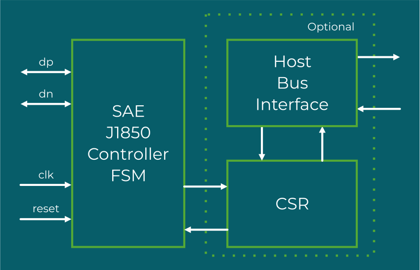
Designed to address the full breadth of SAE J1850 controller requirements, the IP supports all four frame formats, hardware CRC generation and checking, multi-byte transmit and receive, BREAK symbol generation, and collision detection with dedicated symbol timing adjustment registers. Its interrupt-driven transmit completion notification and comprehensive symbol support give automotive ECU teams a production-tested, spec-complete J1850 controller that integrates cleanly into diagnostic tool, body control module, and legacy powertrain communication designs.

Built for design flexibility and silicon efficiency, the IP core is highly configurable for both ASIC and FPGA implementations, with a strong focus on area optimization, power management, and peak performance. Its parameterized architecture and clean host interface enable fast integration and confident design bring-up across a wide range of automotive process nodes and target applications.
Request Data Sheet
SAE J1850 Controller
Key Features
  • Full SAE J1850 Controller Functionality – Complete J1850 implementation per SAE J1850-2015 supporting both VPW (10.4 kbps single-wire) and PWM (41.6 kbps dual-wire differential) bus implementations
  • All Frame Format Support – Type 0, 1, 2, and 3 J1850 frame formats supported for complete protocol coverage across all J1850 application profiles
  • Hardware CRC – Hardware CRC generation and checking per SAE J1850-2015 specification for reliable, low-overhead frame integrity verification
  • Multi-Byte Transmit and Receive – Multi-byte frame transmission and reception for complete J1850 message handling
  • BREAK Symbol Generation – J1850 BREAK symbol generation for bus reset and network management operations
  • Collision Detection – Hardware collision detection for reliable multi-master bus arbitration in shared J1850 network topologies
  • Symbol Timing Adjustment – Dedicated register for symbol timing adjustments for precise, application-specific J1850 bus timing calibration
  • Interrupt-Driven Operation – IRQ generation after frame transmission completion for efficient, event-driven host controller integration
Compliance and Compatibility
  • Fully compliant with SAE J1850-2015 Class B Data Communication Network Interface specification
  • Supports both J1850 VPW (single-wire, 10.4 kbps) and J1850 PWM (dual-wire differential, 41.6 kbps) physical layer implementations
  • Configurable SoC interface supporting AMBA AXI, AHB, APB, and custom wrappers for seamless integration
  • Compatible with ASIC and FPGA design flows across leading foundry process nodes
  • Compatible with all major EDA synthesis, simulation, and linting flows

Request Datasheet